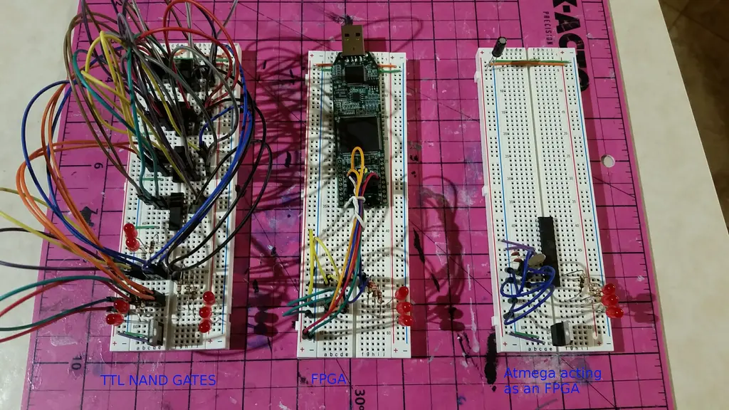
Designing hardware logic circuits can be fun. The old school way to do this was with NAND gates, on a bread board, wired up with jumper wires. This is still possible, but it doesn’t take much before the number of gates gets out of hand. A newer option is to use an FPGA (Field Programmable Gate Array). These chips can rewire themselves to become any digital logic circuit you can design, but aren’t cheap and readily available. I will show how this FPGA can be replaced with a cheap Atmega chip from an Arduino UNO, effectively putting the digital circuit into a DIP package, which is very breadboard friendly.
Step 1: Design the Circuit That the “FPGA” Will Represent

I will build a 2 bit + 2 bit adder. It takes two pairs of logic input pins, and outputs one triplett of output pins.
To do this with NAND gates, see the schematic in the picture. It needs 14 NAND gates. I used 4 quad NAND gate TTL chips, and wired them up on the bread board.
I added some LEDs (don’t forget the current limiting resistors) to show when the input and output pins were on (high), and when they were off (low). To drive the input pins, I either jumpered them to the ground rail or the positive power rail.
This circuit works, but it already takes up 4 TTL chips, and is a rat’s nest of wires. If more bits were needed, there would be more bread boards, and more jumpers. Very quickly the size of the circuit would get out of hand.
On a side note, when working with TTL gates, they do not output exactly 0V or 5V as one would expect. They often output around 3V for “high”, but the exact voltage is in a very wide range. The same circuit using the CMOS equivalent chips would have better exactly 0V to exactly 5V swings.
Step 2: Enter the FPGA

An FPGA is a fantastical chip, that can literally become any combination of logic gates, wired together in any combination. One designs the “circuit” in a hardware design language (HDL). There are multiple such languages, one of which is called Verilog. The .v file in the picture is the Verilog equivalent of the two bit adder. The .pch file below it is also needed to assign the input and output pins named in the verilog file to real hardware pins on the chip.
In this case I am using a Lattice Semiconductors iCEstick development board (http://www.latticesemi.com/icestick). The actual FPGA chip is a iCE40HX-1k, with a little over 1000 gates, which can each become any logic gate. That means each gate can be a NAND gate, or an OR gate, NOT gate, NOR, XOR, etc. Additionally each gate can handle more than two inputs. This is specific to each manufacturer, but on the iCE40’s each gate can handle 4 inputs. Thus each gate is vastly more capable than the 2 input NAND gates.
I had to assign the 4 input pine and the 3 output pins to physical pins 91, 90, 88, 87, 81, 80, and 79 respectively. This is specific to the fpga chip and the breakout board it is on, and how those pins are wired to the PMOD port. This is available in the datasheets for this FPGA board.
Lattice provides their own tool chain to synthesize (the FPGA equivalent to compilation for CPUs) circuits from Verilog, but I used the free open source tool chain icestorm (http://www.clifford.at/icestorm/). The installation instructions are available on that site. With icestorm installed, and the verilog and pcf file, the commands to load this circuit onto the FPGA are:
yosys -p “synth_ice40 -blif twoBitAdder.v” twoBitAdder.blif
arachne-pnr -d 1k -p iCEstick.pcf twoBitAdder.blif -o twoBitAdder.asc
icepack twoBitAdder.asc twoBitAdder.bin
iceprog twoBitAdder.bin
This works great, but including shipping this iCEstick will cost about $30. This isn’t the cheapest way to build a digital circuit, but It is powerful. It has over 1000 gates and for this tiny circuit it only uses 3 of them. The NAND gate equivalent used 14 gates. This is due to the fact that each gate can become any kind of gate, and each gate is actually a 4 input gate. Each gate can do more. If you need more gates, the iCEstick has a bigger brother with 8000 gates, that costs about double. Other manufacturers have other offerings but the price can get quite steep.
Step 3: From FPGA to Arduino

FPGAs are great, but can be expensive, hard to come by, and aren’t very bread board friendly. A breadboard friendly and cheap chip is the Atmega 328 P, which comes in a neat DIP package, perfect for breadboarding. It also can be had for around $4. This is the heart of the Arduino UNO. You could of course use the whole UNO, but be cheap, we can pull the Atmega 328 P off the UNO, and use it by itself. I did use the UNO board as a programmer for the Atmega though.
At this point you will need
1. An Arduino UNO, with the removable Atmega 328P CPU.
2. Another Atmega 328P with the Arduino bootloader pre-burned, to replace the one we are about to take out of the UNO. (Optional assuming you still want to have a useable UNO).
The goal is to convert the verilog file into an arduino project that can be loaded into the 328P. Arduino is based on C++. Conveniently there is a translator from Verilog to C++, called Verilator (https://www.veripool.org/wiki/verilator). Verilator is intended to be used by hardware designers who need to simulate their designs before committing those designs to expensive hardware. Verilator cross compiles the verilog to C++, then the user provides a test harness to provide simulated input signals and record the output signals. We are going to use it to cram the verilog design into the Atmega 328P using the Arduino tool chain.
First install Verilator. Follow the instructions at https://www.veripool.org/projects/verilator/wiki/I…
Also install the Arduino IDE, and test that it can connect to the Arduino UNO over USB.
We will be using the same verilog file as for the FPGA, except that the names of the pins needs to be changed. I added an underscore (_) to the beginning of each. This is needed because the arduino libraries include a header file that translates things like B0, B001, etc, to binary numbers. The other input pin names would have been fine as-is, but B0 and B1 would have caused the build to fail.
In the directory containing twoBitAdder.v and iCEstick.pcf, run the following:
verilator -Wall –cc twoBitAdder.v
This will create a subdirectory called obj_dir containing several new files. We only need the header and cpp files, VtwoBitAdder.h, VtwoBitAdder.cpp, VtwoBitAdder__Syms.h, and VtwoBitAdder__Syms.cpp.
In the Arduino IDE, create a new sketch called twoBitAdder.ino. This will create the ino file in a new directory also called twoBitAdder, inside your Arduino sketchbook directory. Copy your VtwoBitAdder.h and VtwoBitAdder.cpp files to this twoBitAdder folder in your Arduino folder.
Now copy the header files from the verilator installation.
cp /usr/local/share/verilator/include/verilated* .
finally copy in the std c++ library in from https://github.com/maniacbug/StandardCplusplus . Per their installation instructions “This is installed just like a regular Arduino library. Unpack the contents of the distribution into the ‘libraries’ folder under your sketchbook. For example, my sketchbook is at /home/maniacbug/Source/Arduino, so this library is in /home/maniacbug/Source/Arduino/libraries/StandardCplusplus .
Be sure to reset your Arduino IDE after installing it.”
Now replace the content of twoBitAdder.ino with the one provided on this step. This is a test harness that verilator expects, which sets up the input/output pins, then in the loop, reads the input pins, feeds them to the VtwoBitAdder (the translated version of our circuit), then reads the outputs from VtwoBitAdder and applies them to the output pins.
This program should compile and execute on the Arduino UNO.
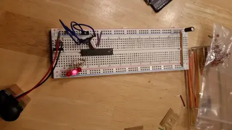
Step 4: From Arduino to DIP Chip on a Bread Board.
Now that the program is running on the Arduino, we no longer need the Arduino board itself. All we need is the CPU.
Remove the Atmega 328P carefully from the Arduino UNO socket, and optionally insert its replacement.
Put the Atmega 328P onto the breadboard. Put the end with the divot pointing up on the bread board. Pin 1 is the top left pin. Pin 2 is the next one down, and so on to pin 14 which is at the bottom left. Then pin 15 is bottom right, and pins 16 to 28 count back up the right side of the chip.
Connect pins 8 and 22 to ground.
Connect pin 7 to VCC (+5V).
Connect a 16Mhz quartz crystal between pins 9 and 10. Also a small capacitor (22pF) between pin 9 and ground, and between pin 10 and ground. This gives the Atmega 328P the 16Mhz clock speed. There are instructions elsewhere on teaching the 328P to instead use its internal 8Mhz clock which would save a couple parts, but that would slow down the processor.
The Arduino GPIO ports 5,6,7, and 8, which we used for the input pins are actually the physical pins 11, 12, 13, 14 on the Atmega 328P. That would be the four bottom pins on the left.
The Arduino GPIO ports 11, 10, and 9, which we used for the output pins are actually the physical pins 17, 16, 15 on the Atmega 328P. That would be the bottom three pins on the right.
I hooked up the LEDs to these pins as before.
Step 5: Conclusion

TTL chips work, but it takes a lot of them to build anything. FPGAs work really well, but aren’t cheap. If you can live with fewer IO pins, and lower speed, then an Atmega 328P may be the chip for you.
Some things to keep in mind:
FPGA:
Pro
– Can handle high speed signals. Because there is no CPU to bottleneck processing down to one instruction at a time, the limiting factor is the propagation delay through the gates on the given circuit. In many cases this may be much faster than the clock provided with the chip. For my design, the computed delay would have allowed for the twoBitAdder to respond to about 100 million changes in input values per second (100Mhz) even though the on-board clock is only a 12Mhz crystal.
– As the design gets more complex the performance of the existing circuits does not degrade (much). Because adding circuits to the fabric is simply putting something new in unused real-estate, it does not impact existing circuitry.
– Depending on the FPGA, the number of available IO pins can be very high, and they generally are not locked into any particular purpose.
Con
– Can be expensive and/or hard to come by.
– Usually comes in a BGA package that requires some kind of breakout board to work with the chip in any amateur project. If you are building it into a design with a custom multi-layer SMT PCB, this isn’t a problem.
– Most FPGA manufacturers provide their own closed source design software, which in some cases may cost money, or have a license expiration date.
Arduino as an FPGA:
Pro
– Cheap, and easy to get. Just search for atmega328p-pu on Amazon. They should be about $4/piece. Several sellers sell them in lots of 3 or 4.
– This is a DIP package, meaning in fits perfectly on a breadboard with its external pins.
– This is a 5V device, which can make interfacing with other 5V devices easy.
Con
– The ATMEGA328P has a limited number of IO pins (23), and several of them are reserved for specific tasks.
– As the circuit complexity increases, the amount of code run in the Arduino loop method increases, meaning the duration of each cycle is longer.
– Even if the complexity of the circuit is low, each cycle requires many CPU instructions to fetch the input pin values, and write output pin values, and return to the top of the loop. With a 16Mhz crystal, even at one instruction per clock cycle, the loop won’t run more than maybe 1 million times per second (1Mhz). For most amateur electronics projects that is way faster than needed though.